Electronic Modular Control Panel II+ Paralleling (EMCP II+P) Page 117
Systems Operation Troubleshooting Testing and Adjusting
KENR8601 117
Troubleshooting Section
Results:
•
OK – The resistance is greater than 5000 ohms.
The problem may be intermittent.
Repair: Use the System Schematic and examine
the wiring between the GSC+P and the ALM for
nicks, abrasion, or other damage. Refer to Testing
And Adjust ing , “Schematics and Wiring Diagram s”.
STOP.
•
NOT OK – The resistance is NOT greater than
5000 ohms. The ALM has failed.
Repair: Replace the ALM.
STOP.
i02888202
GSC CID 0334 - FMI 03
SMCS Code: 4490-035
Conditions Which Generate This Code:
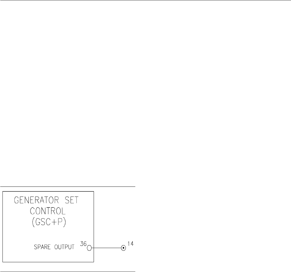
g01437849
Illustration 70
System schematic for the spare output
The spare output on the GSC+P is strictly for the use
of customers. The spare output is programmable in
order to activate under a variety of conditions. The
default parameter programming causes the GSC+P
to activate the output when the engine is in cooldown
mode. The GSC+P treats a CID 0334 FMI 03 as an
alarm fault. For more information, refer to Systems
Operation, “Spare Input/Output Programming OP6”.
The customer and/or the dealer are responsible for
documenting and troubleshooting any connections
to this output.
The voltage on the spare output is approximately
5.0 DCV when there are no connections and when
the spare output is not active. When the spare
output is active, the voltage on the sp are o utput is
approximately 0 volts. The spare output is capable of
drawing (sinking) approximately 100 mA.
The possible cause of a CID 0334 FMI 03 is a short
from the positive terminal of the battery (“BATT+”) to
the spare output signal.
Troubleshooting of a spare output fault is direct. The
FMI de fines the fault. FMI 03 occurs when the spare
outputisshortedto“BATT+”.Inordertofind the exact
cause of the fault, use the following information.
•
FMI information
•
system schematic of spare output
•
documentation of the customer
•
documentation of the dealer
Tes t Step 1. CHECK THE GENERATOR
SET CONTROL
A. Verify that the CID 0334 FMI 03 diagnostic code
is active.
B. Disconnect the wire from pin 36 of the GSC+P.
C. Measure the voltage between pin 36 of the
GSC+P and frame ground.
Expected Result:
The voltage is approximately 5 ± 1.0 DCV.
Results:
•
OK – The voltage is approximately 5 ± 1.0 DCV.
The voltage is correct. Proceed to test step 2.
•
NOTOK –ThevoltageisNOTapproximately5±
1.0DCV.ThevoltageisNOTcorrect.TheGSC+P
has failed.
Repair: It is unlikely that the GSC+P has failed.
Exit this diagnostic code procedure and repeat
the CID 0334 FMI 03 diagnostic code procedure
again. If the cause of the failure is still unknown,
then replace the GSC+P.
STOP.
Test Step 2. CHECK FOR A SHORT TO
“BATT+” IN THE WIRING OF THE SPARE
OUTPUT
A. Disconnect the negative battery terminal
“(BATT-)”.
B. Disconnect the wire from pin 36 of the GSC+P.
C. Disconnect the other end of the wire at the
customer device.
Contents Summary of Electronic Modular Control Panel II+ Paralleling (EMCP II+P)
- Page 1KENR8601 January 2008 Systems Operation Troubleshooting Testing and Adjusting Electronic Modular Control Panel II+ Paralleling (EMCP II+P) SXC1-Up (Generator Set) For C32 Generator Set Packaged in Griffin, GA
- Page 2i01658146 Important Safety Information Most accidents that involve product operation, maintenance and repair are caused by failure to observe basic safety rules or precautions. An accident can often be avoided by recognizing potentially hazardous situations before an accident occurs. A person must b
- Page 3KENR8601 3 Table of Contents Table of Contents Diagnostic Code Procedures Troubleshooting Diagnostic Codes ....................... 90 GSC CID 0100 - FMI 02 ....................................... 92 GSC CID 0110 - FMI 02 ........................................ 93 Systems Operation Section GSC CID 0
- Page 44 KENR8601 Table of Contents Relay Module - Replace ..................................... 170 EMCP Electronic Control (Generator Set) - Replace ............................................................. 171 EMCP Electronic Control (Generator Set) - Flash Program ..................................
- Page 5KENR8601 5 Systems Operation Section Systems Operation Section i02897558 General Information SMCS Code: 4490 g00730400 Illustration 1 Block diagram of a generator set with EMCP II+
- Page 66 KENR8601 Systems Operation Section i02902082 Component Location SMCS Code: 4490 g01444598 Illustration 2 Control Panel (1. ) Generator Set Control with Paralleling (6) Speed Adjust Potentiometer (SAP) (11) Circuit Breaker Open Push button (GSC+P) (7) Either Starting aid (ES) (CBOPB) indicator ligh
- Page 7KENR8601 7 Systems Operation Section g01444726 Illustration 3 Relay panel
- Page 88 KENR8601 Systems Operation Section (1) AC Circuit Breaker (AC-CB1) (11) System in Auto Relay (SIAR) (19) Run Relay (RR) (2) AC Control Relay (AC-CR2) (12) Diode (20) Dead Bus Permissive Relay (DBPR) (3) Off/Reset Relay (ORR) (13) Voltage Regulator Alarm Relay (VRAR) (21) Load Shed/add Relay (LSR)
- Page 9KENR8601 9 Systems Operation Section i02897579 • The displays show the fault codes. The displays also show the information for programming that EMCP Electronic Control is used by the GSC+P. (Generator Set) • The GSC+P monitors the system for faults. If a SMCS Code: 4490 fault occurs, the GSC+P provi
- Page 1010 KENR8601 Systems Operation Section GSC+P Serial Number The yellow spare fault indicators (2) FLASH when the conditions that are associated with that spare fault are active. The three spare faults can be programmed to show coolant loss, oil temperature, spare fault condition or no assignment. The
- Page 11KENR8601 11 Systems Operation Section Low Oil Pressure – The engine oil pressure drops Upper Display below the setpoints for low oil pressure shutdown that are programmed into the GSC+P. There are two low oil pressure setpoints. One setpoint is used when the engine is at idle speed. The other setpoi
- Page 1212 KENR8601 Systems Operation Section Lower Display g00527266 Illustration 10 Upper Display Showing: g00394557 Illustration 14 480 volts, line to line voltage of phase A to phase B Lower Display (6) With All Segments 60 hertz, generator frequency 1000 amperes, total line current of phase A The lower
- Page 13KENR8601 13 Systems Operation Section • Total reactive energy output (kVARHr) Note: All real power values are signed with a “+” or a “−”. A negative value indicates reverse power. Note: Real power phase A, B, and C as well as power factor phase A, B, and C are not shown when setpoint P032 is set to
- Page 1414 KENR8601 Systems Operation Section • Left side exhaust temperature (optional) Keypad • Right side exhaust temperature (optional) • Engine oil temperature (optional) • System battery voltage • Engine hours g00395398 Illustration 24 • Engine speed Keypad (7) for the EMCPII+P Control Panel • Engine
- Page 15KENR8601 15 Systems Operation Section Alarm Codes Key – If fault alarm indicator (4) is FLASHING, pressing this key causes upper display (5) to show the corresponding alarm fault code. Pressing this key again will resume the showing of generator AC output information on the upper display (5). If fau
- Page 1616 KENR8601 Systems Operation Section Table 1 • When the relay is active the normally open contacts Load Specifications For GSC+P Relay Module close. Relay Module Terminal Rating For Rating For • When the relay is inactive the normally closed Number Resistive Inductive contacts close. Loads Loads RM
- Page 17KENR8601 17 Systems Operation Section i02897868 Instrument Panel SMCS Code: 4490; 7451 g01443947 Illustration 27 Instrument Panel Switches (1) Engine Control Switch (ECS) (4) Circuit Breaker Open Push button (7) Ether Starting Aid Switch (ES) (2) Emergency Stop Push button (ESTOP) (CBOPB) (8) Speed
- Page 1818 KENR8601 Systems Operation Section i02897869 i02897891 Data Link Sensors SMCS Code: 4490 SMCS Code: 4490 The GSC+P monitors the following engine sensors that are listed below. • Liquid Level Sensor (Engine Coolant) for all engines • Optional Temperature Sensor (Engine Oil) for all engines • Speed
- Page 19KENR8601 19 Systems Operation Section The engine oil temperature sensor is a pulse width There are three setpoints that are related to the loss modulated type of sensor. The sensor continuously of engine coolant. The setpoints are programmed generates a PWM signal. The duty cycle of the into the GSC
- Page 2020 KENR8601 Systems Operation Section i02897960 Modes Of Operation SMCS Code: 4490 Table 2 Display Area Functions When In Normal Mode, Alarm Mode Or Shutdown Mode(1) Item Of Display Area Normal Mode(2) Alarm Mode(2) Shutdown Mode Upper Display AC Data Shown AC Data Shown(3) Fault Code Shown Lower Di
- Page 21KENR8601 21 Systems Operation Section Service Mode – The GSC+P goes into Service Mode when the operator presses the “Service Mode” key that is located on the keypad. The operator can use Service Mode for the following purposes: • Assist with troubleshooting diagnostic faults. • Verify, calibrate or
- Page 2222 KENR8601 Systems Operation Section Note: The optional Customer Communication 6. The engines’ ECM deactivates the starting motor Module (CCM) can remotely control certain generator relay when the engine speed has reached the set functions. This remote control can only occur crank terminate speed.
- Page 23KENR8601 23 Systems Operation Section 6. When the engine speed reaches zero rpm, the Note: When the operator overrides a shutdown fault GSC+P deactivates the Crank Terminate Relay to be an alarm fault, the corresponding dedicated (CTR) and a restart is now allowed. fault shutdown indicator is on con
- Page 2424 KENR8601 Systems Operation Section i02897993 Note: The spare output may also be programmed to activate when a shutdown occurs. This output can Shutdown Mode drive a relay in order to open the circuit breaker, or the output can open a transfer switch. Refer to System SMCS Code: 4490 Operation, “Sp
- Page 25KENR8601 25 Systems Operation Section i02898014 Note: The GSC+P is not intended for use with DELTA WIRED GENERATORS. If setpoint P032 is set to 1 Paralleling Mode (delta generators), the synchroscope will flash as shown in illustration 34. An “AL17” diagnostic code SMCS Code: 4490 will appear when t
- Page 2626 KENR8601 Systems Operation Section Table 3 EMCP +P Parallel Functions Parallel Function Bus Status ECS Position Parallel Control GSC+P Close Breaker Switch Position Frequency Output Control Automatic Live Start or Auto(1) Auto Controls frequency, When Synchronization brings generator in synchroni
- Page 27KENR8601 27 Systems Operation Section Dead Bus Relay – The Dead Bus Relay (DBR) that indicates the state of the bus The normally closed contacts are closed when the bus is dead, and the level of the GSC+P dead bus sensor input is battery negative. A live bus is indicated by an inactive level floatin
- Page 2828 KENR8601 Systems Operation Section Synchronizing Tuning Procedure During synchronization, the GSC+P continuously monitors the frequency and the phase angle of the Due to the variance in the characteristics of the incoming voltage of the generator and the bus. The engine and the characteristics of
- Page 29KENR8601 29 Systems Operation Section 5. Place the PCS in the AUTO position. Place the 13. Turn the PCS to the OFF position. Place the ECS ECS in the AUTO position. The GSC+P will adjust in the COOLDOWN position. Enter Service Mode the engine speed to the frequency of the bus. Wait and select OP11 S
- Page 3030 KENR8601 Systems Operation Section 4. The first generator set to energize VBR will initiate e. The generator set has reached 90% rated the dead bus close sequence and will inhibit the speed and voltage, as indicated by the VBR. other generator set from closing to the dead bus. If the first genera
- Page 31KENR8601 31 Systems Operation Section Manual Synchronization Mode 6. When the output frequency is in phase with the bus frequency and within the phase tolerance limit Dead Bus Close (P305), the GSC+P will issue a breaker close command. 1. For manual synchronization, the PCS must be in the MANUAL pos
- Page 3232 KENR8601 Systems Operation Section Service Mode has options that can be selected. Note: The appropriate “Scroll” Key should be held Service personnel use the options to obtain down in order to rapidly scroll through a large range information about the generator set, and the operator of informatio
- Page 33KENR8601 33 Systems Operation Section Options OP4 through OP11 of the Service Mode When an active diagnostic code changes to an require a password. Password entry reduces the inactive diagnostic code, the GSC+P will function in possibility of mistakenly altering information. OP3 the following manner
- Page 3434 KENR8601 Systems Operation Section 6. Press “EXIT” key. “OP 1” is showing on lower GSC+P Serial Number – The serial number of the display. GSC+P has ten digits. This number is unique for each GSC+P. The serial number is stamped on a 7. Press “EXIT” key. The display is now in normal label on the b
- Page 35KENR8601 35 Systems Operation Section 3. Press “SELECT” key. “P001” is showing for OP2-0 Note: Any active shutdown fault must be made which is followed by the value of the setpoint. inactive in order to access Service Mode. A shutdown “P101” is showing for OP2-1 which is followed fault is active if
- Page 3636 KENR8601 Systems Operation Section i02898183 4. Press and hold the “ENTER” key for two seconds. If there is only one CID FMI fault code, the CID Fault Log Clearing OP4 FMI fault that was flashing disappears and the upper display is blank except for the flashing SMCS Code: 4490 “SERV” indicator. “
- Page 37KENR8601 37 Systems Operation Section Note: Any active shutdown fault must be made inactive in order to access service mode. When a shutdown fault is active, a shutdown indicator is FLASHING. To temporarily change a shutdown fault from an active shutdown fault to an inactive shutdown fault, turn the
- Page 3838 KENR8601 Systems Operation Section Table 6 OP5-0 Setpoints - Engine/Generator Programming(1) Setpoint Name Description Range Of Value Controller Default P001 Fuel Solenoid Type of fuel system solenoid used on the 0 - ETR fuel solenoid 0 Type generator set. All Larne-built generators 1 - ETS fuel
- Page 39KENR8601 39 Systems Operation Section (Table 6, contd) OP5-0 Setpoints - Engine/Generator Programming(1) Setpoint Name Description Range Of Value Controller Default P014(3) Low Oil Pressure Oil pressure used by the GSC+P to declare 20 to 336 kPa 70 kPa (10 psi) Shutdown At Idle that a low oil pressu
- Page 4040 KENR8601 Systems Operation Section (Table 6, contd) OP5-0 Setpoints - Engine/Generator Programming(1) Setpoint Name Description Range Of Value Controller Default P027 Shutdown GSC+P responds to an engine high oil 0 - alarm only 0 Override temperature fault. (Determined by application (shutdown ov
- Page 41KENR8601 41 Systems Operation Section 2. Press “SCROLL UP” key two times. “OP5-1” is showing on the lower display. 3. Press “SELECT” key once. “P101” is showing. “P101” is followed by the value of the setpoint. 4. Press the “SCROLL UP” key or the “SCROLL DOWN” key. The next setpoint is showing with
- Page 4242 KENR8601 Systems Operation Section (Table 7, contd) OP5-1 Setpoints (1) - Protective Relaying Programming Setpoint Name Description Range Of Value Factory Default P109 Undervoltage Alarm Amount of time the GSC+P waits 0 to 120 seconds(2) in increments 10 Time Delay before inssuing an undervoltage
- Page 43KENR8601 43 Systems Operation Section (Table 7, contd) OP5-1 Setpoints (1) - Protective Relaying Programming Setpoint Name Description Range Of Value Factory Default P120 Underfrequency Alarm Frequency the GSC+P uses to issue MUI Engines: 30 to 50, for 50 Hz 45 Hz Threshold an underfrequency alarm.
- Page 4444 KENR8601 Systems Operation Section (Table 7, contd) OP5-1 Setpoints (1) - Protective Relaying Programming Setpoint Name Description Range Of Value Factory Default P135 Phase Overcurrent Amount of time the GSC+P waits 0 to 250 seconds(2) in increments 30 Shutdown Time Delay before issuing a phase
- Page 45KENR8601 45 Systems Operation Section Table 8 OP5-3 Setpoints - Paralleling Programming Setpoint Name Description Range Of Value Factory Default P301 Synchronization Enables or disables the synchronization 0 - disabled 0 Enable function, and specifies the type of Load 1 - Woodward Share control bein
- Page 4646 KENR8601 Systems Operation Section i02898429 Spare Input/Output Programming OP6 SMCS Code: 4490 OP6 is the option for the programming of the following parameters: Spare Inputs, Spare Indicators, Spare Outputs, and Programmable Spare Relay Outputs. These spare inputs and outputs are provided in or
- Page 47KENR8601 47 Systems Operation Section Alarm Mode Sequence Of Operation – If a fault Spare Output occurs in a spare input that is programmed as an active input, the following steps occur and the fault is programmed as an alarm fault: 1. The GSC+P waits until the time delay elapses. 2. The fault alarm
- Page 4848 KENR8601 Systems Operation Section The GSC+P must be programmed to accept the When the outputs are triggered, the GSC+P must be condition that triggers the spare output to the active programmed to decide whether the outputs of the state. A large selection of trigger conditions is PSR are active o
- Page 49KENR8601 49 Systems Operation Section 5. Press the “SELECT” key. The value of the setpoint is flashing. 6. Press the “SCROLL UP” key or the “SCROLL DOWN” key in order to adjust the value of the setpoint. 7. Press the “ENTER” key. The value of the setpoint stops flashing. Repeat steps 4, 5, 6, and 7
- Page 5050 KENR8601 Systems Operation Section (Table 9, contd) OP6-0 Setpoints(1) - Spare Input/Output Programming Setpoint Name Description Range Of Value Factory Default SP13 Spare Output GSC+P response 0 - active low 0 Response to the spare output 1 - active high trigger condition. SP15 Spare Relay Outpu
- Page 51KENR8601 51 Systems Operation Section i02898745 Voltmeter/Ammeter Programming OP8 SMCS Code: 4490 Table 10 OP8 Setpoints(1) - Voltmeter Ammeter Programming Setpoint Name Description Range Of Value Factory Default AC01 Phase A (VA) Voltage Calibration value used by the GSC+P to compensate for 0 to 25
- Page 5252 KENR8601 Systems Operation Section 1. Turn the ECS to the STOP position in order to P003 Shutdown Override For Engine Fault – shut down the engine. Enter service mode and P003 is the GSC+P response to a low engine oil enter the password. OP 4 is showing on the lower pressure. P003 is also the res
- Page 53KENR8601 53 Systems Operation Section Procedure For Overspeed 5. The setpoint value that is flashing on the upper display is increased by pressing the “SCROLL Verification UP” key. With each press of the “SCROLL UP” key, the setpoint value increases by five. Press Note: Service mode cannot be access
- Page 5454 KENR8601 Systems Operation Section i02898780 AC Offset Adjustment OP10 SMCS Code: 4490 Table 11 OP10 Setpoints(1) - AC Offset Adjustment Setpoint Name Description Range Of Value Factory Default PH A Phase A Voltage Value used by the −5.0% to +5.0% of 0 Adjustment GSC+P in order to measured voltag
- Page 55KENR8601 55 Systems Operation Section Note: The adjusted voltages are used for the display i02898801 only. The adjusted voltages will not be sent over the CAT Data Link to other modules. The customer Parallel Setpoint Tuning OP-11 communication module is another module that may receive information o
- Page 5656 KENR8601 Systems Operation Section 10. Press the “EXIT” key. The display returns to the SP Fault Codes – The SP fault codes are shown as Normal Mode. SP1 through SP4 on the upper display. Diagnostic Codes – Diagnostic codes are shown i02898889 as numeric values. Diagnostic codes are identified by
- Page 57KENR8601 57 Systems Operation Section AL2 Low Water Temperature Alarm – When the AL5 Low Engine Coolant Level Fault – When the engine coolant temperature decreases to setpoint engine coolant level drops below the probe of the P016, the GSC+P issues a low water temperature coolant loss sensor for ten
- Page 5858 KENR8601 Systems Operation Section When the fault is programmed as a shutdown fault, AL9 Generator Over Frequency Fault (protective the fault shutdown indicator will FLASH and the AL7 relaying function) – When the generator frequency fault code is immediately shown on the upper display. rises abo
- Page 59KENR8601 59 Systems Operation Section AL11 Generator Reverse Power Fault (protective When the fault is programmed as an alarm fault, the relaying function) – When reverse power rises fault alarm indicator will FLASH and the AL13 fault above the P126 setpoint, the GSC+P issues a code is shown on the
- Page 6060 KENR8601 Systems Operation Section AL16 Incorrect Phase Sequence – This fault AL18 Synchronizer Time-out Alarm – This fault occurs whenever any synchronization function occurs whenever the GSC+P is unable to complete is in progress, and the GSC+P verifies that the Automatic Synchronization or Dea
- Page 61KENR8601 61 Systems Operation Section i02899086 i02899114 SP Fault Codes Diagnostic Codes SMCS Code: 4490 SMCS Code: 4490 SP fault codes are associated with the spare inputs. Diagnostic fault codes are associated with failed SP fault codes are either alarm faults or shutdown electrical components or
- Page 6262 KENR8601 Systems Operation Section Control System Identifier – The control system The GSC+P has a fault log to help with identifier is a single digit. The control system that can troubleshooting of diagnostic faults. Inactive generate a diagnostic code is the GSC+P. diagnostic fault codes (CID FM
- Page 63KENR8601 63 Systems Operation Section Note: The GSC+P diagnoses a fault in the spare i02899223 output circuit. Refer to Testing and Adjusting, “CID 448, FMI 12 Programmable Spare Relay Failed-Test” Programmable Kilowatt Level for more information. Output i02899172 SMCS Code: 4490 Programmable Spare
- Page 6464 KENR8601 Systems Operation Section i02899242 The Alarm Module (ALM) gives a warning of conditions that are becoming a problem. The warning Alarm Modules occurs before conditions are severe enough to shut down the engine. SMCS Code: 4490 An alarm fault develops while the generator set is running a
- Page 65KENR8601 65 Systems Operation Section 6. Coolant temperature has exceeded the high Indicator And Horn Operation water temperature shutdown setpoint that is programmed into the GSC+P. Table 12 Indicator And Horn Function 7. The engine has failed to start(overcrank fault). Indicator NFPA 99 ALM EMCP R
- Page 6666 KENR8601 Systems Operation Section When an alarm fault occurs, the corresponding indicator flashes. The indicator flashes at two hertz and the horn sounds. If the alarm fault is NOT LATCHED the indicator turns off when the alarm fault ceases. The horn also turns off when the alarm fault ceases. I
- Page 67KENR8601 67 Systems Operation Section i02899457 Table 14 Alarm Module Control Connections For Customer Alarm Module (Custom) Screw Terminal Signal Name 1 “BATT+” SMCS Code: 4490 2 Not Used 3 Input 5 - Indicator 5 (Red) 4 Input 6 - Indicator 6 (Red) 5 Input 7 - Indicator 7 (Red) 6 Input 8 - Indicator
- Page 6868 KENR8601 Systems Operation Section When an input that is corresponding to one of the red i02899482 indicators is activated, the indicator will flash and the horn will sound. When the input is disconnected from Customer Interface Module the battery negative terminal, the horn will continue to soun
- Page 69KENR8601 69 Systems Operation Section • Low oil pressure shutdown • Connections that may be used by the customers at the relay board (1) are 6-32 screw terminals. • High coolant temperature shutdown i02899537 • Overcrank System Communication • Overspeed Module (Customer) • Diagnostic fault (GSC+P) S
- Page 7070 KENR8601 Systems Operation Section • Activate or deactivate the Electronic Governor Relay (EGR), provided that the low oil pressure shutdown setpoint has been exceeded. • Activate the GFR or deactivate the GFR, provided that the GSC+P has not detected a fault. In this case, the GSC+P will already
- Page 71KENR8601 71 Troubleshooting Section Troubleshooting Section Do not connect generator to a utility electrical dis- Introduction tribution system unless it is isolated from the sys- tem. Electrical feedback into the distribution sys- tem can occur and could cause personal injury or i02897272 death. Ge
- Page 7272 KENR8601 Troubleshooting Section i02897282 Fault Identification SMCS Code: 4490-035 Table 16 Fault Identification Indicator Fault Code on upper DIAG Indicator left side of GSC+P display Fault Type Refer to Topic Fault Alarm CID FMI(1) Flashing Active Alarm Troubleshooting Diagnostic Codes SP1, SP
- Page 73KENR8601 73 Troubleshooting Section 6. Go to the third column in the chart which describes the status of “DIAG” indicator (8). 7. Read the last two columns in order to find the type of fault and corresponding topic within this module. g00614724 Illustration 50 GSC+P Display Area (1) Dedicated shutdo
- Page 7474 KENR8601 Troubleshooting Section Symptom Procedures • Programming Error - Fault Is Overridden Or Disabled: It is possible to program the GSC+P in order to override certain shutdown faults. An i02895174 overridden shutdown fault will be treated as an alarm fault. The YELLOW fault alarm indicator w
- Page 75KENR8601 75 Troubleshooting Section • NO – The GSC+P does NOT show a diagnostic Repair: Check the appropriate setpoints for code on the upper display. Proceed to Test Step 2. correct values. In order to view the setpoints, refer to System Operation, “Engine/Generator Test Step 2. CHECK THE YELLOW FA
- Page 7676 KENR8601 Troubleshooting Section Repair: The GSC+P Relay Module may have Repair: Troubleshoot and repair the wiring. Refer failed. It is unlikely that the GSC+P Relay Module to Generator Set Wiring Diagram in Testing And has failed. Exit this procedure and perform this Adjusting, “Schematics And
- Page 77KENR8601 77 Troubleshooting Section g01436567 Illustration 52 System Schematic For An AC Transformer Box (ATB+) A Wye Connection Is Shown For The Generator. Test Step 1. THE PROBLEM IS WITH AC VOLTAGE OR THE PROBLEM IS WITH When the engine-generator, or any source to AC CURRENT. which the engine-gen
- Page 7878 KENR8601 Troubleshooting Section Test Step 2. CHECK THE FUSES. Test Step 4. CHECK THE CONNECTIONS A. Check the three fuses on the AC Transformer Box A. Shut down the engine. + (ATB+). B. Check the harness connector and the terminals of Expected Result: the ATB+. The fuses should not be open. C. C
- Page 79KENR8601 79 Troubleshooting Section Repair: The ATB+ has failed. Replace the Expected Result: ATB+. Refer to Testing and Adjusting Section, “EMCP Electronic Control (AC Transformer Box) The resistance should be approximately 5 Ohms. - Replace”. Results: STOP. • OK – The resistances are approximately
- Page 8080 KENR8601 Troubleshooting Section Results: Repair: The ATB+ has failed. Replace the ATB+. Refer to the Testing and Adjusting Section, • OK – The wires in the harness for the GSC+P “EMPC Electronic Control (AC Transformer Box) measure less than 5 Ohms. - Replace”. Repair: The ATB+ has failed. Repla
- Page 81KENR8601 81 Troubleshooting Section i02884572 Display of Voltage or Current or Power Is Inaccurate SMCS Code: 4490-035 System Operation Description: g00481725 Illustration 53 Block diagram of AC voltage display in the EMCP II +P g01436567 Illustration 54 System schematic for AC Transformer Box + (AT
- Page 8282 KENR8601 Troubleshooting Section Table 17 Selection of AC Voltage Range Input When the engine-generator, or any source to Voltages which the engine-generator is synchronized to, is External GSC+P for AC GSC+P operating, voltages up to 600V are present in the Potential P020 Trans- Internal Jumper
- Page 83KENR8601 83 Troubleshooting Section Expected Result: Results: The power consumption that is displayed on the • YES – The jumper is installed correctly in order GSC+P should be accurate. to match the value in setpoint P020. Proceed to Test Step 6. Results: • NO – The jumper is NOT installed correctly
- Page 8484 KENR8601 Troubleshooting Section Repair: Program the setpoints in OP8 to match the Repair: Program P021 tothe same ratio as values on the ATB+. Refer to System Operation, the current transformers. Refer to Testing “Voltmeter/Ammeter Programming OP8”. and Adjusting, “Engine/Generator Setpoint Prog
- Page 85KENR8601 85 Troubleshooting Section Repair: Program the setpoints in OP8 to match the values on the ATB+. Refer to System Operation, “Voltmeter/Ammeter Programming OP8”. STOP. Test Step 10. INACCURATE POWER CONSUMPTION IS DISPLAYED ON THE GSC+P. A. Start the genset. B. Check for inaccurate power fac
- Page 8686 KENR8601 Troubleshooting Section Test Step 11. CHECK THE POLARITY OF THE CURRENT TRANSFORMERS g01438390 Illustration 55 A. Turn the ECS to the STOP position in order to shut down the engine. B. Check the polarity of the current transformers. Refer to Illustration 55. Expected Result: The polarity
- Page 87KENR8601 87 Troubleshooting Section i02885949 Indicators of Alarm Module or Remote Annunciator Are Constantly Flashing SMCS Code: 4490-035 System Operation Description: g01438113 Illustration 56 System schematic for Alarm Module (ALM) The fault indicators of the remote annunciator or the • Verify Th
- Page 8888 KENR8601 Troubleshooting Section • Check The Type Of Wire Or Cable On The Test Step 2. CHECK THE ALARM Remote Modules. Three separate wires for the MODULE FOR FAULTS. following connections are recommended for remote installations: The positive battery wire (“BATT+”), A. The indicators on the alar
- Page 89KENR8601 89 Troubleshooting Section Results: • OK – The diagnostic codes occur. The GSC+P has not failed. The wire from GSC+P contact 35 to terminal 2 of the alarm module is open or the wire has failed. Repair: Repair the wire or replace the wire. STOP. • NOT OK – The diagnostic codes do not occur.
- Page 9090 KENR8601 Troubleshooting Section Diagnostic Code The GSC+P has a fault log to help with troubleshooting of diagnostic codes. Inactive Procedures diagnostic codes (CID FMI) are recorded in the fault log for viewing at a later time. Also, the number of occurrences are totalled and the number of i02
- Page 91KENR8601 91 Troubleshooting Section Diagnostic Codes (Table 18, contd) Diagnostic Codes(1) Table 18 Diagnostic Codes(1) CID No. / FMI No. Description FMI 12 Failed component CID No. / FMI No. Description CID 442 - Generator Fault Relay: CID 100 - Pressure Sensor (Engine Oil): FMI 12 Failed component
- Page 9292 KENR8601 Troubleshooting Section (Table 18, contd) i02897294 Diagnostic Codes(1) GSC CID 0100 - FMI 02 CID No. / FMI No. Description SMCS Code: 1924-035 CID 1168 - Dead Bus Sensor: Conditions Which Generate This Code: FMI 3 Voltage above normal This diagnostic code is for the pressure sensor FMI
- Page 93KENR8601 93 Troubleshooting Section Expected Result: System Response: There is a letter “E” after the number of the CID that Note: The GSC+P is usually programmed to treat is on the upper display panel of the EMCP II+P. a problem with the coolant temperature sensor as an alarm fault. Setpoint P004 i
- Page 9494 KENR8601 Troubleshooting Section Expected Result: The EMCPII+P system monitors engine coolant in order to protect the engine in case of a coolant The resistance that was measured between pin 19 temperature problem. The engine coolant loss and pin 20 is less than 5 ohms. function is an option that
- Page 95KENR8601 95 Troubleshooting Section Expected Result: Expected Result: The voltage should be 8.0 DCV (± 0.5 DCV). CID 111 FMI 3 should no longer appear on the upper display. Results: Results: • OK – The voltage is 8.0 DCV (± 0.5 DCV). Proceed to Test Step 2. • OK – CID 111 FMI 3 no longer appears on
- Page 9696 KENR8601 Troubleshooting Section D. Measure the resistance of the ground circuit. The Repair: Start the engine. If the CID 111 FMI 3 is still ground circuit is from pin “B” of the sensor harness showing, the GSC+P may have failed. It is unlikely connector to pin “31” of the GSC+P harness that the
- Page 97KENR8601 97 Troubleshooting Section g01447141 Illustration 60 The EMCP II+P monitors the battery voltage in order to protect the EMCP II+P from a battery problem or from a charging problem. The battery voltage is received from the engine ECM by the CAT data link. If you receive a CID 168 E fault, re
- Page 9898 KENR8601 Troubleshooting Section Table 19 POSSIBLE CAUSES FOR CID 168 DIAGNOSTIC CODES The Location that the Diagnostic Code Battery Voltage Thresholds Battery Voltage Thresholds Diagnostic Code is (24 Volt System) (32 Volt System) Displayed On Engine ECM CID 168 E 00 The engine is running and th
- Page 99KENR8601 99 Troubleshooting Section Repair: Proceed to Testing and Adjusting, Expected Result: “Charging System - Test”. The voltage that was measured between the “BATT+” STOP. and “BATT-” terminals and the voltage that was measured measured between the GSC-RM2 and Test Step 2. COMPARE THE VOLTAGE “
- Page 100100 KENR8601 Troubleshooting Section Results: Results: • OK – The measured resistances match the Table. • OK – The voltages are within 2.0 VDC of each Proceed to Test Step 5. other. The fault is probably an intermittent fault which is caused by a faulty connector. Inspect the • NOT OK – The measured
- Page 101KENR8601 101 Troubleshooting Section Repair: Reprogram the GSC+P. Refer to System The GSC+P treats a CID 190 FMI 2 as a shutdown Operation, “Engine Generator Programming fault. The engine is not allowed to crank or the OP5-0”. engine is not allowed to run when a CID 190 FMI 2 diagnostic code is acti
- Page 102102 KENR8601 Troubleshooting Section Expected Result: F. Check for a short circuit. Check the resistance from pin “1” to pin “2” of the GSC+P harness CID 190 FMI 2 should not appear on the upper connector. The resistance should be greater than display. 5000 ohms. Results: Expected Result: • OK – CID
- Page 103KENR8601 103 Troubleshooting Section Results: Repair: It is unlikely that the GSC+P has failed. Exit this procedure and perform this procedure • OK – The shield is securely fastened. The again. If the diagnostic code is still present, replace connection between the sensor and the mating the GSC+P. R
- Page 104104 KENR8601 Troubleshooting Section The possible causes of a CID 190 FMI 3 are listed below. • There is an open in the signal circuit. Clear the diagnostic code from the fault log after troubleshooting is complete. Test Step 1. CHECK THE HARNESS AND THE SPEED SENSOR. A. Turn the Engine Control Swit
- Page 105KENR8601 105 Troubleshooting Section B. At the connector of the sensor, measure the Results: resistance between pin “1” and pin “2”. • OK – The harness functions properly. Proceed to Expected Result: Test Step 5. The resistance should be between 100 to 350 ohms. • NOT OK – The harness wiring with th
- Page 106106 KENR8601 Troubleshooting Section Expected Result: Test Step 8. CHECK THE SIGNAL VOLTAGE. No damage should be present. A. This is an additional check of the circuit. Make sure Results: that all of the harness connectors are connected. • OK – No damage is present. Reinstall the engine B. Use a mul
- Page 107KENR8601 107 Troubleshooting Section Results: • OK – The resistance between the disconnected positive battery cable and either of the CAT Data Link wires is greater than 5000 ohms. Proceed to Test Step 2. • NOT OK – The resistance between the disconnected positive battery cable and either of the CAT
- Page 108108 KENR8601 Troubleshooting Section i02887665 Note: The GSC+P setpoints must be programmed in the OFF/RESET position when a shutdown fault is GSC CID 0268 - FMI 02 active. If the alarm for the fault indicator is FLASHING the GSC+P can be programmed with the ECS in the SMCS Code: 4490-035 OFF/RESET
- Page 109KENR8601 109 Troubleshooting Section • Systems Operation, “Voltmeter/Ammeter Table 21 Programming OP8” Sensor MUI EUI PEEC Engines Engines Engines STOP. Coolant Yes No Yes Temperature i02896489 Oil Pressure Yes No Yes GSC CID 0269 - FMI 03 Coolant Loss Yes Yes Yes SMCS Code: 4490-035-NS Oil Temperat
- Page 110110 KENR8601 Troubleshooting Section D. Observe the upper display for the CID 0269 FMI 03. Expected Result: The CID 0269 FMI 03 should not be showing. The diagnostic code should be inactive. Results: • OK – The CID 0269 FMI 03 is not showing. The GSC+P is functioning properly. Therefore, the engine
- Page 111KENR8601 111 Troubleshooting Section The possible cause of a CID 0269 FMI 04 occurs E. Press the “Alarm Codes” key. when the voltage of the sensor supply is less than 7.5 DCV. F. Observe the upper display for the CID 0269 FMI 04. Begin performing these procedures only when CID 0269 FMI 04 is active
- Page 112112 KENR8601 Troubleshooting Section Repair: Repair the engine harness or replace the engine harness. STOP. i02887983 GSC CID 0333 - FMI 03 SMCS Code: 4490-035 Conditions Which Generate This Code: g01438113 Illustration 68 System Schematic For Alarm Module (ALM) The Alarm Module (ALM) is available a
- Page 113KENR8601 113 Troubleshooting Section One possible cause of a CID 0333 FMI 03 diagnostic Results: code is a short to the positive battery terminal (“BATT+”). • OK – The resistance is correct. Proceed to Test Step 3. The GSC+P treats a CID 0333 FMI 03 as an alarm fault. Clear the diagnostic code from
- Page 114114 KENR8601 Troubleshooting Section Results: • YES – The diagnostic code is NOT active. The diagnostic code does not exist at this time. Repair: The initial diagnostic code was probably caused by a poor electrical connection or a short at one of the harness connectors that was disconnected and reco
- Page 115KENR8601 115 Troubleshooting Section i02888018 GSC CID 0333 - FMI 04 SMCS Code: 4490-035 Conditions Which Generate This Code: g01438113 Illustration 69 System Schematic For Alarm Module (ALM) The Alarm Module (ALM) is available as an option. Note: Diagnostic codes are created when the The ALM may be
- Page 116116 KENR8601 Troubleshooting Section Test Step 1. CHECK IF THE DIAGNOSTIC Repair: The GSC+P may have failed. It is unlikely CODE IS ACTIVE that the GSC+P has failed. Exit this procedure and perform this procedure again. Replace the GSC+P A. Turn the Engine Control Switch (ECS) to the if the CID 0333
- Page 117KENR8601 117 Troubleshooting Section Results: The possible cause of a CID 0334 FMI 03 is a short from the positive terminal of the battery (“BATT+”) to • OK – The resistance is greater than 5000 ohms. the spare output signal. The problem may be intermittent. Troubleshooting of a spare output fault i
- Page 118118 KENR8601 Troubleshooting Section D. Measure the resistance from the wire that was disconnected from pin 36 of the GSC+P to “BATT+” of the GSC+P. Expected Result: The resistance is greater than 5000 ohms. Results: • OK – The resistance is greater than 5000 ohms. The circuit is correct. 3 • NOT OK
- Page 119KENR8601 119 Troubleshooting Section i02888284 GSC CID 0334 - FMI 04 SMCS Code: 4490-035 Conditions Which Generate This Code: g01438113 Illustration 71 System schematic for the spare output The spare output on the GSC+P is strictly for the use Troubleshooting of a spare output fault is direct. The o
- Page 120120 KENR8601 Troubleshooting Section Expected Result: C. Turn the ECS to STOP and check if the diagnostic code is still active. The voltage is approximately 5 ± 1.0 DCV. Expected Result: Results: The diagnostic code is not active. • OK – The voltage is approximately 5 ± 1.0 DCV. The voltage is corre
- Page 121KENR8601 121 Troubleshooting Section i02888312 GSC CID 0336 - FMI 02 SMCS Code: 7332-035 Conditions Which Generate This Code: g01437916 Illustration 72 Simplified schematic for The Engine Control Switch (ECS) The Engine Control Switch (ECS) is used by the “AUTO” – The engine starts and the engine ru
- Page 122122 KENR8601 Troubleshooting Section “COOLDOWN/STOP” – The engine maintains rated D. At the GSC+P harness connector, measure the speed for the cooldown period. The cooldown period resistance from pin “39” to “BATT-” of the relay is programmable from 0 to 30 minutes. After the module. Measure the res
- Page 123KENR8601 123 Troubleshooting Section Results: Repair: Repair the harness wiring or replace the harness wiring. Repair the wiring or replace • OK – The resistance measurements are correct. the wiring between the “BATT-”, the ECS, and Proceed to Test Step 3. the GSC+P connector. Reconnect the remote s
- Page 124124 KENR8601 Troubleshooting Section Test Step 5. CHECK IF THE DIAGNOSTIC i02890206 CODE IS STILL ACTIVE GSC CID 0441 - FMI 12 A. Clean the contacts of the harness connectors. Refer to Testing and Adjusting, “Electrical SMCS Code: 4490-035-R7 Connector - Inspect”. Conditions Which Generate This Code
- Page 125KENR8601 125 Troubleshooting Section This troubleshooting procedure is for an active CID Results: 0441 FMI 12 code. Also, this procedure is for an inactive CID 0441 FMI 12 code. • OK – The cable is firmly seated in the connector. The clamp is in place. The cable is not damaged. Test Step 1. CHECK TH
- Page 126126 KENR8601 Troubleshooting Section Repair: Replace the relay module. Refer toTesting C. Observe the upper display. Check that the CID And Adjusting, “Relay Module - Replace”. 0442 FMI 12 is active. STOP. D. If the diagnostic code is not active, enter the Service Mode. View the fault log for a OP1.
- Page 127KENR8601 127 Troubleshooting Section Repair: Replace the clamp if the clamp is missing. i02888449 If the cable is damaged, replace the GSC+P. Refer to Testing and Adjusting, “EMCP Electronic Control GSC CID 0443 - FMI 12 (Generator Set) - Replace”. SMCS Code: 4490-035-R7 STOP. Conditions Which Gener
- Page 128128 KENR8601 Troubleshooting Section C. Observe the upper display. Check that the CID Repair: Replace the clamp if the clamp is missing. 0443 FMI 12 is active. If the cable is damaged, replace the GSC+P. Refer to Testing and Adjusting, “EMCP Electronic Control D. If the diagnostic code is not active
- Page 129KENR8601 129 Troubleshooting Section i02890172 Expected Result: GSC CID 0445 - FMI 12 A CID 0445 FMI 12 is displayed as an active diagnostic code or CID 0445 FMI 12 is displayed as SMCS Code: 4490-035-R7 an inactive diagnostic code. Conditions Which Generate This Code: Results: The Run Relay (RR) is
- Page 130130 KENR8601 Troubleshooting Section B. Reconnect the negative battery cable. Expected Result: C. Disconnect all wires from RM-23 and RM-24 of The resistance measurement from RM-23 to RM-9 the relay module. should be greater than 5000 ohms. The resistance measurement should be less than 5 ohms at RM
- Page 131KENR8601 131 Troubleshooting Section • If a CID 0446 FMI 12 occurs and the ASR is not Expected Result: activated, then there is no immediate effect on the system. The engine is able to start and the engine The cable should be firmly seated in the connector. is able to run. The clamp should be in pla
- Page 132132 KENR8601 Troubleshooting Section • NOT OK – Either one of the resistance Test Step 1. CHECK THE STATUS OF THE measurements are NOT correct. The relay module DIAGNOSTIC CODE. has failed. A. Turn the Engine Control Switch (ECS) to the Repair: Replace the relay module. Refer to Testing OFF/RESET po
- Page 133KENR8601 133 Troubleshooting Section Results: Repair: Replace the relay module. Refer to Testing And Adjusting, “Relay Module - Replace”. • OK – The cable is firmly seated in the connector. The clamp is in place. The cable is not damaged. STOP. Reassemble the relay module to the GSC+P. Proceed to Te
- Page 134134 KENR8601 Troubleshooting Section • If a CID 0448 FMI 12 occurs and the PSR is C. Temporarily, remove the relay module from the inactive, any customer’s equipment that is wired to GSC+P. Refer to Testing And Adjusting, “Relay RM-25 will remain deactivated and any customer’s Module - Replace”. equ
- Page 135KENR8601 135 Troubleshooting Section Results: Repair: The GSC+P is operating normally. • OK – The resistance measurements are correct. STOP. The problem does not exist at this time. The initial problem was probably caused by a poor i02890397 electrical connection or a short at one of the harness con
- Page 136136 KENR8601 Troubleshooting Section The GSC+P treats a CID 0566 FMI 07 as a Results: shutdown fault. Clear the fault from the fault log after troubleshooting is complete. • YES – The air shutoff solenoid can be activated and the air shutoff solenoid can be deactivated. Note: This procedure requires
- Page 137KENR8601 137 Troubleshooting Section i02889768 Clear the diagnostic code from the fault log after troubleshooting is complete. The GSC+P is usually GSC CID 0590 - FMI 09 programmed to treat a CID 590 diagnostic code as an “alarm fault”. Setpoint P04 is 0. If the GSC is SMCS Code: 1901-035 programmed
- Page 138138 KENR8601 Troubleshooting Section Note: The GSC+P cannot detect an open in the D. Measure the resistance between pin 21 and circuit of the CCM data link. The GSC+P treats a “BATT-”. CID 0770 as an alarm fault. Active alarm faults are shown on the display when the “Alarm Codes” key Expected Result
- Page 139KENR8601 139 Troubleshooting Section For Automatic Synchronization, the output of Test Step 2. CHECK THE ACTIVE the close breaker control is pulsed active for a VOLTAGE LEVEL OF THE CLOSE programmed period of time. The period of time is BREAKER OUTPUT. set according to setpoint P302. While the condi
- Page 140140 KENR8601 Troubleshooting Section i02901402 Results: GSC CID 0858 - FMI 04 • OK – The voltage measures 5.2 ± 1.0 DCV. The voltage is correct. Proceed to test step 2. SMCS Code: 1420-035 • NOT OK – The voltage is below 5.2 ± 1.0 DCV. Conditions Which Generate This Code: Repair: The GSC+P may have
- Page 141KENR8601 141 Troubleshooting Section Repair: The GSC+P may have failed. It is unlikely The possible cause of a CID 0859 FMI 3 is a short that the GSC+P has failed. Exit this procedure and from the positive battery terminal circuit (“BATT+”) to perform this entire procedure again. If the problem the
- Page 142142 KENR8601 Troubleshooting Section D. Measure the resistance between the wire that was The kW level output will be activated whenever disconnected from pin 34 of the GSC+P and pin the total power output of the generator exceed 10 of the kW relay. the setpoint P139. The kW level output is the pin 3
- Page 143KENR8601 143 Troubleshooting Section Results: i02890649 • OK – The diagnostic code changes to inactive. GSC CID 1038 - FMI 03 Proceed to Test Step 2. SMCS Code: 1264-035 • NOT OK – The diagnostic code remains active. The GSC+P may have failed. Conditions Which Generate This Code: Repair: It is unlik
- Page 144144 KENR8601 Troubleshooting Section Repair: The GSC+P may have failed. It is unlikely C. Perform the Automatic paralleling function. that the GSC+P has failed. Exit this procedure and If necessary, refer to Systems Operation, perform this entire procedure again. If the problem “Synchronization Tuni
- Page 145KENR8601 145 Troubleshooting Section The possible cause of a CID 1038 FMI 04 is a short D. Allow the voltage to stabilize. Use a cable probe from the output signal of the “Speed Adjust 1” to the to measure the voltage on pin 27 of GSC+P. negative battery terminal. Expected Result: A CID 1038 FMI 04
- Page 146146 KENR8601 Troubleshooting Section Repair: The GSC+P may have failed. It is unlikely C. Use a cable probe to measure the voltage at pin that the GSC+P has failed. Exit this procedure and 25 of the GSC+P. perform this entire procedure again. If the problem remains, replace the GSC+P. Refer to Testi
- Page 147KENR8601 147 Troubleshooting Section Repair: The GSC+P is operating correctly, and B. Locate the wire that is connecting pin 29 of the problem is in the wiring or the component that the GSC+P to terminal “DBR-9” of the Dead is connected to the input of the circuit breaker Bus Relay (DBR). Remove thi
- Page 148148 KENR8601 Troubleshooting Section Test Step 3. CHECK THE FUNCTION OF A CID 1168 FMI 04 is detected under the following THE BUS RELAY. condition. A. Carefully reconnect any power wires of the DBR • The voltage of the Phase A of the bus is greater that may have previously been removed. than 50% of
- Page 149KENR8601 149 Troubleshooting Section Expected Result: i02891171 The voltage of pin 29 of the GSC+P should measure GSC CID 1169 - FMI 02 0.0 ± 0.5 DCV. SMCS Code: 1409-035 Results: Conditions Which Generate This Code: • OK – The voltage is 0.0 ± 0.5 DCV. Proceed to Test Step 3. The “ATB+” reduces the
- Page 150150 KENR8601 Troubleshooting Section Repair: Use the ATB+ System Schematic and Test Step 1. CHECK THE PHASE the AC Schematic in the Schematics And Wiring ANGLE OF THE INPUTS TO THE BUS Diagrams section to troubleshoot the wiring and TRANSFORMER BOX (BTB +) find the exact cause of the problem. A shor
- Page 151KENR8601 151 Troubleshooting Section Expected Result: C. Start the engine. The engine is running at rated speed. The voltage between “B1” and “B2” of the generator is the same as the line to line voltage. D. Measure the voltage between pin 17 and pin 18 of the GSC+P connector. Note: If external pote
- Page 152152 KENR8601 Troubleshooting Section Test Step 6. CHECK THE BTB+ OUTPUT Test Step 1. CHECK THE VOLTAGE CIRCUIT OF THE INPUTS TO THE BUS TRANSFORMER BOX (BTB +) A. Stop the engine. B. Disconnect three terminal connector J1 on the BTB+. C. Measure the resistance from pin A to pin B of J1. Expected Res
- Page 153KENR8601 153 Troubleshooting Section • NOT OK – The voltage measured from Phase A • NOT OK – The voltage measured from pin 17 and and Phase C to the neutral lead is NOT greater 18 to the negative battery terminal is NOT greater than 55% to 60% of the voltage measured from than 55% to 60% of the volt
- Page 154154 KENR8601 Troubleshooting Section • NOT OK – The fuses are blown. Repair: There is no voltage on phase C. Use the System Schematic for the BTB + and the AC Repair: Replace the fuses. schematic in Testing And Adjusting, “Schematics And Wiring Diagrams” section to troubleshoot the STOP. wiring and
- Page 155KENR8601 155 Troubleshooting Section Expected Result: The voltage should be equal to the voltage measured in Test Step 2 divided by 15 ± 2% (14.7 to 15.3). Results: • OK – The voltage is correct. CID 1170 FMI 2 is still active. Repair: The GSC+P may have failed. It is unlikely that the GSC+P has fai
- Page 156156 KENR8601 Troubleshooting Section Diagnostic System Procedures i02892285 AL Fault Code SMCS Code: 4490-035 Table 23 AL Fault Code Troubleshooting AL Fault Code Description Troubleshooting AL1 High Water Temperature Alarm Refer to the Troubleshooting, “Troubleshooting Coolant temperature increases
- Page 157KENR8601 157 Troubleshooting Section (Table 23, contd) AL Fault Code Troubleshooting AL Fault Code Description Troubleshooting AL13 Generator Total Overcurrent Fault Check for a cause of the overcurrent. Check Total current rises above the P131 or P136 setpoint P029 and setpoints P128 through P137.
- Page 158158 KENR8601 Troubleshooting Section Table 24 Spare Fault Codes Spare GSC+P Terminal Related Fault Code Connector Strip Setpoints(1) Pin SP1 23 N/A SP01, SP02, Spare Fault 1 SP03 SP2 24 N/A SP04, SP05, Spare Fault 2 SP06 SP3 25 N/A SP07, SP08, Spare Fault 3 SP09 SP4 29 N/A SP10, SP11, Illustration 8
- Page 159KENR8601 159 Troubleshooting Section 5. Check the wiring to the corresponding spare fault • High Water Temperature input for an unwanted short. The short can be to the negative battery terminal (“BATT-”). Also, • Engine Overspeed The short can be to the positive battery terminal (“BATT+”). • Overcra
- Page 160160 KENR8601 Troubleshooting Section Test Step 2. CHECK THE EMERGENCY i02893433 STOP INDICATOR. Indicator for High Water Note: The following procedure will create diagnostic Temperature codes. Clear these created diagnostic codes after troubleshooting is complete. SMCS Code: 4490-035-IND A. The ECS
- Page 161KENR8601 161 Troubleshooting Section Results: i02895157 • OK – The coolant level is at the proper level. Indicator for Low Oil Pressure Proceed to Test Step 2. SMCS Code: 4490-035-IND • NOT OK – Coolant level is not correct. Reference: The engine Electronic Control Module Repair: Find the cause and
- Page 162162 KENR8601 Testing and Adjusting Section Testing and Adjusting Intermittent electrical problems are often caused by poor connections. Always check for an active Section diagnostic code before breaking any connections. Also, always check for an active diagnostic code after the connector is reconnec
- Page 163KENR8601 163 Testing and Adjusting Section g01135980 Illustration 87 Correct way to route a harness and insert a plug g00690571 g00828600 Illustration 88 Illustration 89 Proper Installation of Plug DT Type sealing plug The 8T-8729 Connector Pin (2) and the 8T-8730 Connector Socket (1) is designed to
- Page 164164 KENR8601 Testing and Adjusting Section a. Ensure that the connector is properly locked. a. Each connector contact should withstand 45 N Also, ensure that the two halves of the (10 lb) of pull. Each wire should remain in the connector can not be pulled apart. connector body. This test checks whet
- Page 165KENR8601 165 Testing and Adjusting Section Results: Expected Result: All of the connectors should be completely coupled and all of the seals OK – The wires are free of abrasion, nicks, should be completely inserted. The harness or cuts and the harness is properly clamped. and the wiring should be fr
- Page 166166 KENR8601 Testing and Adjusting Section Results: OK – The pin contacts and the socket contacts appear to be OK. STOP. NOT OK – A problem exists with the connector terminal. Repair: Replace the connector contact. STOP. i02916819 Alarm Module Control - Adjust SMCS Code: 4490-025 g00838765 Illustrat
- Page 167KENR8601 167 Testing and Adjusting Section Adjustment Procedure i02916844 1. Gain access to the rear of the ALM. Removal of Speed Sensor (Engine) - Adjust the ALM is not necessary unless removing the ALM is needed for access. All wiring remains SMCS Code: 1907-025 connected to the terminals of the A
- Page 168168 KENR8601 Testing and Adjusting Section i02900007 6. Reconnect the harness connector to the ATB+. Reconnect all the wires to the terminal strip that EMCP Electronic Control (AC were removed. Reconnect the positive lead wire Transformer Box) - Replace to the battery. If necessary, refer to the Gen
- Page 169KENR8601 169 Testing and Adjusting Section 3. Disconnect the BTB+ connector from the harness connector. 4. Remove all mounting nuts and mounting screws that fasten the BTB+ to the subpanel. Remove the BTB+. 5. Place the new BTB+ in the subpanel. Install the mounting nuts and mounting screws. Tighten
- Page 170170 KENR8601 Testing and Adjusting Section i02900022 Relay Module - Replace SMCS Code: 4490-510 g00583564 Illustration 95 Replacement Of The Relay Module The Rear View of the GSC+P (1) Relay Module (3) Tape (5) O-Ring Seal (2) Screws (4) Desiccant Package (6) Cable connector Relay module (1) contain
- Page 171KENR8601 171 Testing and Adjusting Section 2. Make sure that all wires at the terminal strips i02900024 of the relay module (1) are marked with the respective termination point. During reassembly EMCP Electronic Control these wires must be reattached to the correct (Generator Set) - Replace terminal
- Page 172172 KENR8601 Testing and Adjusting Section i02900030 EMCP Electronic Control (Generator Set) - Flash Program SMCS Code: 4490-591 Connection Procedure This procedure is used to update the software for generator sets that have an Electronic Modular Control Panel II+P (EMCP II+P) with Generator Set Con
- Page 173KENR8601 173 Testing and Adjusting Section
- Page 174174 KENR8601 Testing and Adjusting Section g00615494 Illustration 96
- Page 175KENR8601 175 Testing and Adjusting Section (1) Relay Module on the GSC+P Control 4. After the start-up is complete, Cat ET will (2) AUX terminal strip automatically try to connect to the GSC+P through (3) 152-7143 GSC Data Cable the communication adapter. (4) Personal Computer (5) 160-0140 PC/COMM A
- Page 176176 KENR8601 Testing and Adjusting Section i02900031 BCF – Battery Charger Failure Switch Typical Generator BTB – Bus Transformer Box Abbreviations BVR – Bus Voltage Relay SMCS Code: 4490 C – Common 52-AX – Circuit Breaker Auxiliary Contact CAM – Custom Alarm Module 52-CC – Circuit Breaker Close Coi
- Page 177KENR8601 177 Testing and Adjusting Section DC – Direct Current GSC+P – Generator Set Control With Paralleling DCT – Droop Current Transformer HZ – Frequency Meter DCV – DC Voltmeter JWH – Jacket Water Heater DS – Disconnect Switch K – Kilowatt ECLC – Engine Coolant Loss Sensor Connector KWR – Kilowa
- Page 178178 KENR8601 Testing and Adjusting Section PCS – Paralleling Control Switch T1/T2/T3 – Phase A/B/C, Generator Side Of Generator Circuit Breaker PF – Power Factor TB – Terminal Block PL# – Panel Illumination Light TSC – Transfer Switch Position Indicating Contact PLS – Panel Light Switch V – AC Voltm
- Page 179KENR8601 179 Testing and Adjusting Section g01443949 Illustration 97
- Page 180180 KENR8601 Testing and Adjusting Section i02916911 Block Diagram of Generator Set Control SMCS Code: 4490; 7566 g00508636 Illustration 98
- Page 181KENR8601 181 Testing and Adjusting Section i02916935 Connector Contact Identification of Generator Set Control SMCS Code: 4490; 7553 g00438305 Illustration 99
- Page 182182 KENR8601 Testing and Adjusting Section i02900025 Schematics and Wiring Diagrams SMCS Code: 7566 NFPA 99 Alarm Module For All Engines g00546229 Illustration 100
- Page 183KENR8601 183 Testing and Adjusting Section Custom Alarm Module For All Engines g00546230 Illustration 101
- Page 184184 KENR8601 Testing and Adjusting Section Load Sharing Module g00688478 Illustration 102
- Page 185KENR8601 185 Testing and Adjusting Section i02906092 Service Record SMCS Code: 4490 Table 26 Service Table - Record Of Setpoint Values Generator Description: Site, Serial No., EMCP II+ Part Number., etc.. Engine /Generator Programming OP5-0 Setpoint Specified Value Actual Value(1) Setpoint Descripti
- Page 186186 KENR8601 Testing and Adjusting Section (Table 26, contd) Service Table - Record Of Setpoint Values Generator Description: Site, Serial No., EMCP II+ Part Number., etc.. Engine /Generator Programming OP5-0 Setpoint Specified Value Actual Value(1) Setpoint Description Possible Values Default Value
- Page 187KENR8601 187 Testing and Adjusting Section (Table 27, contd) Service Table - Record Of Setpoint Values Generator Description: Site, Serial No., EMCP II+ Part Number., etc.. Engine /Generator Programming OP5-0 Setpoint Specified Actual Value(1) Setpoint Description Possible Values Default Value Value
- Page 188188 KENR8601 Testing and Adjusting Section Table 28 Service Table - Record Of Setpoint Values Generator Description : Site, Serial No., EMCP II+ Part No., etc.. OP5-1 Setpoints (1) - Protective Relaying Programming Setpoint Specified Value Actual Value(1) Name Range Of Value Factory Default P101 Ove
- Page 189KENR8601 189 Testing and Adjusting Section (Table 28, contd) Service Table - Record Of Setpoint Values Generator Description : Site, Serial No., EMCP II+ Part No., etc.. OP5-1 Setpoints (1) - Protective Relaying Programming Setpoint Specified Value Actual Value(1) Name Range Of Value Factory Default
- Page 190190 KENR8601 Testing and Adjusting Section (Table 28, contd) Service Table - Record Of Setpoint Values Generator Description : Site, Serial No., EMCP II+ Part No., etc.. OP5-1 Setpoints (1) - Protective Relaying Programming Setpoint Specified Value Actual Value(1) Name Range Of Value Factory Default
- Page 191KENR8601 191 Testing and Adjusting Section (Table 28, contd) Service Table - Record Of Setpoint Values Generator Description : Site, Serial No., EMCP II+ Part No., etc.. OP5-1 Setpoints (1) - Protective Relaying Programming Setpoint Specified Value Actual Value(1) Name Range Of Value Factory Default
- Page 192192 KENR8601 Testing and Adjusting Section Table 29 Service Table - Record Of Setpoint Values OP5-3 Setpoints - Paralleling Programming Generator Description : Site, Serial No., EMCP II+ Part No., etc.. Setpoint Specied Value Actual Value Setpoint Possible Values Default Value Description P301 Synch
- Page 193KENR8601 193 Testing and Adjusting Section Table 30 Service Table - Record Of Setpoint Values Generator Description: Site, Serial No., EMCP II+ Part No., etc.. Setpoint Specified Value Actual Value(1) Setpoint Description Possible Values Default Value Spare Input/Output Programming OP6 SP01 Spare In
- Page 194194 KENR8601 Testing and Adjusting Section (Table 30, contd) Service Table - Record Of Setpoint Values Generator Description: Site, Serial No., EMCP II+ Part No., etc.. Setpoint Specified Value Actual Value(1) Setpoint Description Possible Values Default Value Spare Input/Output Programming OP6 AC05
- Page 195KENR8601 195 Index Section Index A EMCP Electronic Control (Generator Set)............... 9 Fault Indicators .................................................. 10 AC Factory Calibration Setpoint Programming GSC+P Part Number ........................................... 9 OP5-2 .......................
- Page 196196 KENR8601 Index Section GSC CID 0446 - FMI 12 ...................................... 130 Paralleling Mode.................................................... 25 GSC CID 0447 - FMI 12 ...................................... 132 Glossary............................................................. 2
- Page 197KENR8601 197 Index Section Troubleshooting Dedicated Shutdown Indicators ........................................................... 159 Troubleshooting Diagnostic Codes........................ 90 Diagnostic Codes............................................... 91 Troubleshooting Section ............
- Page 198198 KENR8601 Index Section
- Page 199KENR8601 199 Index Section
- Page 200©2008 Caterpillar All Rights Reserved Printed in U.S.A.